In the past days and weeks, there was a lot of talk about Intel’s problems with the next production step in 10 nm. Just recently, Intel had to admit again that it has manufacturing issues at 10 nm and that mass production for desktop and server processors must be postponed again and is now scheduled for sometime in 2019. At yesterday’s 2018 Annual Stockholders’ Meeting, Intel CEO Brian Krzanich had to answer some awkward questions. With the Core i3-8121U a first processor in small series in 10 nm is manufactured, but this is missing on a working graphics unit and so should the also emergent Core m3-8114Y be the first fully functioning desktop processor from this production.
At the 2018 Annual Stockholders’ Meeting, Intel reassured its investors. The next step in 7 nm is not affected by the 10 nm delays. Already used for 14 and 10 nm and thus established technologies are used. But the Extreme Ultraviolet Lithography (EUV or EUVL) is already used in parts. Intel relies mainly on non-native hardware and expects a lot from it:
The production in 10 nm will get as soon as possible under control and sees itself for 7 nm in the plan – at least, this suggests to the outside. Intel is currently shipping its mass-produced products in 14nm and wants to switch to 10nm as soon as possible, and is planning 7nm in real terms. Messages like the start of 7nm mass production at TSMC will work that way, so TSMC is far ahead of Intel’s manufacturing technology.
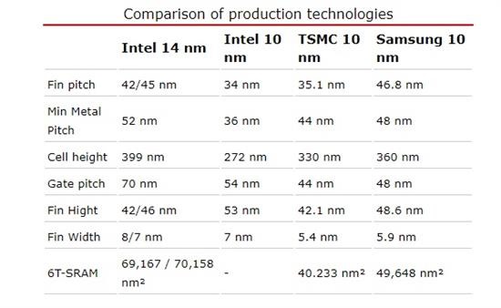
GlobalFoundries as another contract manufacturer is currently shipping for AMD in 14 and 12 nm. Samsung also speaks already of 7 and 5 nm. The contract manufacturers and those with their own factories thus outdo each other regularly. However, data such as 16, 14, 10 or 7 nm are no longer decisive and do not reflect where the advantages of smaller production lie now. Sizes like Fin Pitch, Min Metal Pitch, Cell Height and Gate Pitch.
An important factor is the number of transistors per square millimeter. In this area, Intel is always setting very ambitious goals. With the change of production from 20 to 14 nm, 14 to 10 nm and 10 to 7 nm, the pavers set goals by which factor the packing density should increase. In the case of 20 to 14 nm, this was the factor 2.4 for Intel. With the change from 14 to 10 nm planned Intel with a factor of 2.7, which is apparently also one of the reasons why Intel currently has some difficulties. In order to keep the requirements a bit lower, the goals for the packing density are being reduced and the factor 2.4 is planned again.
Based on the numbers of TSMC and Intel, CLN5, a process in 5 nm, will be a shrink by a factor of 1.8 compared to CLN7FF in 7 nm. Intel is planning 7 nm with a shrink of factor 2.4 of 10 nm. Thus, TSMC is 14 nm at 147 million transistors / mm in 5 nm and Intel at 242 million transistors / mm in 7 nm. Intel’s production in this area is thus significantly further advanced and compact.
TSMC 10nm ~ Intel 14nm. TSMC/Glofo 7nm ~ Intel 10nm. Intel 10nm is a bit denser than 7nm nodes for logic (see image). But 7nm nodes are a bit denser than Intel 10nm for SRAM sizes pic.twitter.com/nymvBwyleu
— juanrga (@juanrga) May 18, 2018
It is becoming increasingly difficult for manufacturers to implement the smaller production steps in practice. However, while Intel is struggling at 10 nm for reasons that are still unknown, the use of EUV will still be a hurdle for all manufacturers. Whether Moores Law is over or not, has been contested for years. The multi-billion investments in new production lines and the development show that the effort is increasing. Just recently, Intel announced that it is investing $5 billion in the expansion of the Fab 28 in Israel.
